Equipment
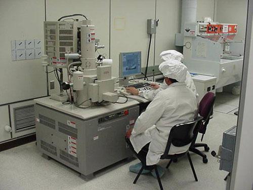
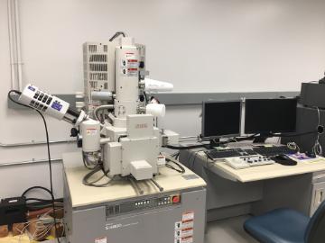
Hitachi S-4800 Field Emission SEM
Description
Field Emission (FE) Scanning Electron Microscope (SEM) is a type of electron microscope that produces images of a sample by scanning it with a focused beam of electrons by an electrostatic field. The most common context is field emission from a solid surface into vacuum. Due to a high vacuum, this unit in particular only allows for dry samples.
The electrons interact with atoms in the sample, producing various signals that can be detected and that contain information about the sample's surface topography and composition. The electron beam is generally scanned in a raster scan pattern, and the beam's position is combined with the detected signal to produce an image. The most common SEM mode is detection of secondary electrons emitted by atoms excited by the electron beam.
The SEM is used particularly for observing the fine structure of a specimen surface at high magnification. Yttrium-Aluminum-Garnet (YAG) backscattered electron (BSE) detector is available to capture contrast-enhanced images of multi-phase materials.
Specifications
| Resolution | Accelerating voltage 15 kV, working distance 4 mm - 1.0 nm Accelerating voltage 1 kV, working distance 1.5 mm - 2.0 nm |
| Magnification |
Magnification: High magnification mode - 100X to 800,000X |
| Electron Optics |
Electron Gun - Cold cathode field emission type |
| Specimen Stage |
Tilt -5 degrees to +70 degrees |
Scanning Transmission Electron Microscope (STEM)
| Specifications: | |
| Resolution | 1.5 nm (with accelerating voltage 30 kV, WD 8 mm and magnification 150,000X) |
| Detector | Scintillator + photomultiplier system |
| Specimen | Thin-sectioned specimen mounted on a 3 mm diameter specimen grid |
| Mode | Bright field image |
Zyvex IC Nanoprober System
| Specifications: | |
| Sample Size | 12 mm diameter |
Oxford EDS (Energy Dispersive Spectroscopy)
Description
Energy Dispersive Spectroscopy (EDS) Analysis provides elemental and chemical analysis of a sample inside the SEM, TEM, or FIB. Oxford Instruments provides Aztec, a new and revolutionary materials characterization system that gathers accurate data at the micro- and nanoscales. EDS provides valuable surface chemical composition and analysis paring with our Hitachi SEM.
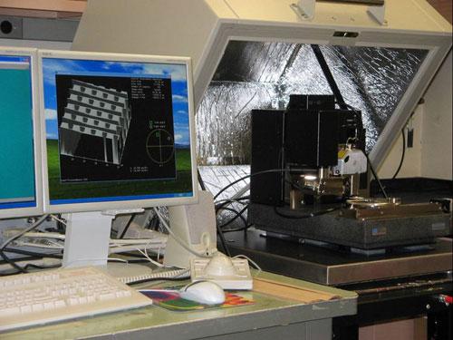
Veeco Dimension 3100 Scanning Probe Microscope (SPM) and Atomic Force Microscope (AFM) System
Description
Atomic-Force Microscopy (AFM) or Scanning-Force Microscopy (SFM) is a high-resolution type of Scanning Probe Microscopy (SPM). The purpose of the AFM allows us to look at individual atoms on the atomic level. Using an AFM, it is possible to measure the roughness of a sample surface at a high resolution to distinguish a sample based on its mechanical properties such as hardness and roughness in addition to perform a microfabrication of a sample (for example, an atomic manipulation).
The AFM can do some things that the SEM cannot do. The AFM can sometimes provide higher resolution than the SEM and does not need to operate in a vacuum. The AFM can operate in ambient air or water, so it can be used to see surfaces of biological samples like living cells.
Specifications
| Resolution | Lateral resolution ~ 5 nm Vertical resolution ~ 1 nm |
| Sample Size | Up to 200 mm diameter and 12 mm thick |
| Mode | Tapping; Contact AFM; Magnetic Force; Electric Force; Force Modulation; Fluid Contact AFM; Fluid Tapping; Tunneling/Conductive AFM |
| Optical System | 410-1845X magnification range Color video camera Motorized zoom system |
CASCADE Microtech Summit 12000 Series Probe Station
Description
Cascade Microtech offers a complete line of high-performance solutions for on-wafer probing, circuit boards and modules, vertical probe cards, MEMS, electro-optic devices and more. A mechanical probe station is used to physically acquire signals from the internal nodes of a semiconductor device. The probe station utilizes manipulators, which allow the precise positioning of thin needles on the surface of a semiconductor device. If the device is being electrically stimulated, the signal is acquired by the mechanical probe and is displayed on an oscilloscope. The mechanical probe station is often used in the failure analysis of semiconductor devices.
There are two types of mechanical probes: active and passive. Passive probes usually consist of a thin tungsten needle. Active probes utilize a FET device on the probe tip in order to significantly reduce loading on the circuit. Mechanical probe stations are often used in academic research on electronics and materials science. It is often faster and more flexible to test a new electronic device or sample with a probe station than to wire bond and package the device before testing.
Specifications
| Stage Size | 200 mm diameter |
| Stage Temp. Range | Ambient to 200 degrees C |
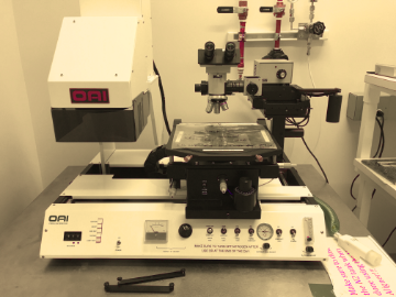
OAI Model 200 Mask Aligner
Description
Mask Aligner is used in photolithographic process. Photolithography is the process of transferring geometric shapes on a mask to the surface of a silicon wafer. The steps involved in the photolithographic process are wafer cleaning; barrier layer formation; photoresist application; soft baking; mask alignment; exposure and development; and hard-baking. Utilizing an innovative, air bearing/vacuum chuck leveling system, the substrate is leveled quickly and gently, for parallel photo mask alignment and uniform contact across the wafer during contact exposure. The system is capable of one micron resolution and alignment precision.
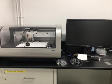
FUJIFILM Dimatix Materials Printer, DMP-2800 Series
Description
This system enables easy printing of structures and samples for process verification and prototype creation. The 3D printer is used for,
- Material and fluid development and evaluation,
- Prototype and sample generation,
- Fluid and substrate interactions evaluation,
- Product development; optimization and evaluation of digital patterns,
- Deposition of biological fluids including cell patterning, DNA arrays, proteomics
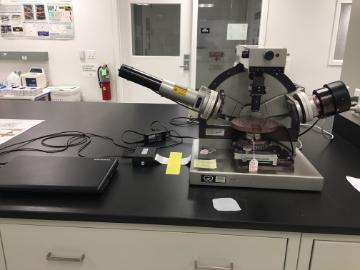
Gaertner Ellipsometer L116B
Description
Ellipsometry is primarily used to determine film thickness and optical constants. However, it is also applied to characterize composition, crystallinity, roughness, doping concentration, and other material properties associated with a change in optical response. It is an obsolete model and only used for a class teaching. On Oct. 2020, The instrument was calibrated, laser replaced, and received a new computer for the program.
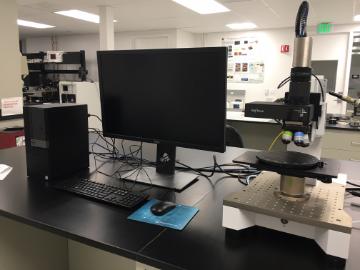
Zeta-20 Optical Profiler
Description
Utilizing ZDot technology, the Zeta-20 images and analyzes surface features on samples of all types: smooth to rough, low reflectivity to high reflectivity, transparent to opaque. Hardware and software options customize the Zeta-20 for specialized measurement needs in 3D imaging. This profiler has a similar function to do what Ellipsometer can do in upgraded functions with 3D imaging.